Difference between revisions of "Xi8088 Version 2.0"
Numberformat (talk | contribs) |
Numberformat (talk | contribs) |
||
| Line 75: | Line 75: | ||
rect 248 29 351 64 [[74F244]] | rect 248 29 351 64 [[74F244]] | ||
</imagemap> | </imagemap> | ||
| + | |||
| + | == Post Assembly == | ||
| + | |||
| + | Once you have your board assembled you can proceed with configuring the memory map. If you plan on using a VGA graphics card and the 128Kb BIOS Flash Chip then all the switches should be in the off position. | ||
== Memory Map == | == Memory Map == | ||
| Line 183: | Line 187: | ||
== Processor Bootstrap == | == Processor Bootstrap == | ||
| − | When the processor starts up it will be looking at fixed memory locations. | + | When the processor starts up it will be looking at fixed memory location. The Intel CPU will be looking at address 0xF:FFF0 for the jump instruction that will tell the processor the location of the POST Entry Point typically this number will be (EA 5B E0). EA is the machine code for JMP FAR absolute 4 byte address specified in the argument. The F000:E05B is the address to jump to. Scrolling up in the window you will see that there is some BIOS code that starts at that point this is the POST entry point which starts with a B8 which is a MOV instruction. |
| + | |||
| + | See table below for these address locations. When burning the BIOS onto the FLASH chip make sure to set the offset from the beginning of the chip since the BIOS is only 32 KiB the offset when using a 128 KiB chip will be 0x18000 I used a TL866 II writer with the XGecu Pro software. You can verify that the last line displayed should begin with EA 5B and end with FC FF. | ||
<pre> | <pre> | ||
Revision as of 18:33, 20 June 2021
Introduction
Xi 8088 IBM PC/XT compatible processor board.
Contributions Welcome
If anyone reading this page is interested in contributing content please send me a text message at 3476042083 with your email address and I will send instructions on how to setup an account.
Features
- ISA board form factor
- Support of PS/2 keyboard and mouse
- Built-in real time clock with NVRAM
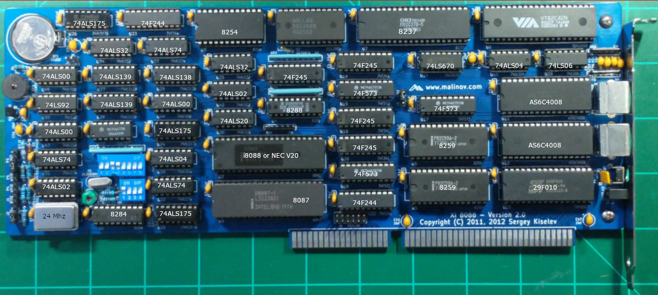
Board Layout
Click on any chip for more information. Most of the chips below lead to blank pages. I am looking for help in populating them with some info. I know datasheets are available however it would be nice to have a brief summary of each component and what is does overall on this board.

Post Assembly
Once you have your board assembled you can proceed with configuring the memory map. If you plan on using a VGA graphics card and the 128Kb BIOS Flash Chip then all the switches should be in the off position.
Memory Map

The 20 bit address bus of the 8088/86 allows 1 Mb of memory space with address range from 00000-FFFFF. During the design phase of the first IBM PC, engineers had to decide n the allocation of the 1-megabyte memory space to various sections of the PC. This memory allocation is called a memory map.
| Start Address | End Address | Size | Purpose | Comments | ||||||||||||||
| 0x00000h | 0x9FFFFh | 640 KiB | Base memory | |||||||||||||||
| 0xA0000h | 0xBFFFFh | 128 KiB | Display memory | |||||||||||||||
| 0xC0000h | 0xEFFFFh | 192 KiB | Upper memory blocks (UMB) and BIOS extension ROMs | Consists of six 32 KiB user configurable blocks, can be either mapped to SRAM (to be used as UMB) or used for BIOS extension ROMs
| ||||||||||||||
|---|---|---|---|---|---|---|---|---|---|---|---|---|---|---|---|---|---|---|
| 0xE0000h | 0xEFFFFh | 64 KiB | On-board BIOS extension ROM | This is the upper 64 KiB of the 192 KiB block seen above. System flash ROM can be mapped here, so it can be used for BIOS extensions
| ||||||||||||||
| 0xF0000h | 0xFFFFFh | 64 KiB | System BIOS | Currently BIOS uses only top 32 KiB of this space (0xF8000h - 0xFFFFFh). The other 32 KiB part is mapped to the flash ROM and can be used for BIOS extensions
|
| Position | Description |
| 8 | ON = Monochrome display (MDA)
OFF = Color display (CGA) |
Processor Bootstrap
When the processor starts up it will be looking at fixed memory location. The Intel CPU will be looking at address 0xF:FFF0 for the jump instruction that will tell the processor the location of the POST Entry Point typically this number will be (EA 5B E0). EA is the machine code for JMP FAR absolute 4 byte address specified in the argument. The F000:E05B is the address to jump to. Scrolling up in the window you will see that there is some BIOS code that starts at that point this is the POST entry point which starts with a B8 which is a MOV instruction.
See table below for these address locations. When burning the BIOS onto the FLASH chip make sure to set the offset from the beginning of the chip since the BIOS is only 32 KiB the offset when using a 128 KiB chip will be 0x18000 I used a TL866 II writer with the XGecu Pro software. You can verify that the last line displayed should begin with EA 5B and end with FC FF.
;-------------------------------------------------------------------------
; Fixed BIOS Entry Points
; Source:
;	Intel(R) Platform Innovation Framework for EFI
;	Compatibility Support Module Specification
;	Section 5.2
;
;	Location	Description
;	--------	-----------
;	F000:E05B	POST Entry Point
;	F000:E2C3	NMI Entry Point
;	F000:E401	HDD Parameter Table
;	F000:E6F2	INT 19 Entry Point
;	F000:E6F5	Configuration Data Table
;	F000:E729	Baut Rate Generator Table
;	F000:E739	INT 14 Entry Point
;	F000:E82E	INT 16 Entry Point
;	F000:E987	INT 09 Entry Point
;	F000:EC59	INT 13 (Floppy) Entry Point
;	F000:EF57	INT 0E Entry Point
;	F000:EFC7	Floppy Disk Controller Parameter Table
;	F000:EFD2	INT 17
;	F000:F065	INT 10 (Video) Entry Point
;	F000:F0A4	INT 1D MDA and CGA Video Parameter Table
;	F000:F841	INT 12 Entry Point
;	F000:F84D	INT 11 Entry Point
;	F000:F859	INT 15 Entry Point
;	F000:FA6E	Low 128 Characters of Graphic Video Font
;	F000:FE6E	INT 1A Entry Point
;	F000:FEA5	INT 08 Entry Point
;	F000:FF53	Dummy Interrupt Handler (IRET)
;	F000:FF54	INT 05 (Print Screen) Entry Point
;	F000:FFF0	Power-On Entry Point
;	F000:FFF5	ROM Date in ASCII "MM/DD/YY" Format (8 Characters)
;	F000:FFFE	System Model (0xFC - AT, 0xFE - XT)
Troubleshooting
Non-Turbo clock is unstable or non existent
Sometimes the non-turbo crystal fails to oscillate. The proposed improvement to this circuit is seen below. I will test it further and introduce this change in the next revision of the board.
For now try out different values of load capacitors. Roughly speaking the formula to determine the values based on the Load capacitance of the crystal (check datasheet) is Cload = c^2/(2c)
For a crystal with load capacitance of 20pf (find in datasheet) then the capacitors you should add up to 40pf. But since capacitors have different tolerances and measuring such small capacitances is hard with cheap equipment then experimenting with different value capacitors is your best bet. Remember that capacitors in parallel add capacitance Cp = c1 + c2... and series they are 1/Cs = 1/c1 + 1/c2 ...